Osaka University, Graduate School of Engineering
Division of Electrical, Electronic and Infocommunications Engineering
Computational Quantum Information Electronics Area

Mori Lab @ Osaka Univ


Our laboratory conducts theoretical research on novel materials and devices, and their applications in large-scale integrated electronic systems. The research topics cover a wide area from the basic semiconductor physics to the circuit and system design.

Atomistic quantum transport simulation of nano-scale transistors

Continual technological innovations in semiconductor industry have made it possible to create metal-oxide-semiconductor field-effect-transistors (MOSFETs) with the channel length down to sub-20 nm. Detailed computational studies are now a necessity to predict the transport characteristics and to accelerate the development of future ultra-small transistors with novel structures and materials, which include three-dimensional device structure, tunnel transistors, compound semiconductors, two-dimensional materials, and so on. We try to obtain a better understanding of quantum transport in nano-scale devices, and develop integrated simulators for next-generation transistors from an animistic view. Our simulators are aimed to run on a massively parallel computing system.

Transport simulation of monolayer devices

Monolayer two-dimensional (2D) materials have attracted much attention because of their possible application in novel electronic devices, such as tunnel field-effect transistors (TFETs). A wide variety of layered materials have been realized, which include graphene, silicene, germanene, and transional metal dicharogonetides (TMDC). We have been developing a carrier transport simulator for such devices including hybrid graphene-quantum dot transistors and in-plane hetero-junction TMDC TFETs.

Advanced modeling and simulation of power devices

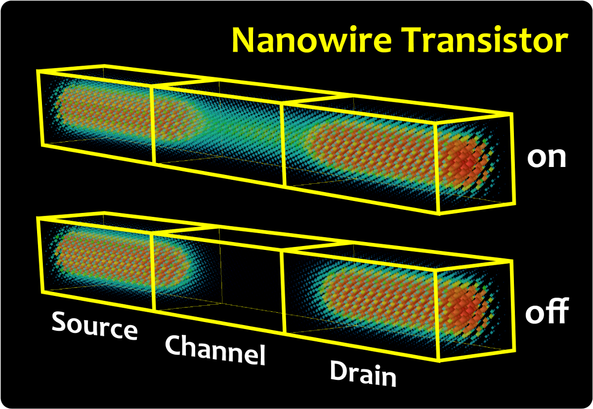
Wide-bandgap (WBG) semiconductors, such as silicon carbide (SiC), gallium nitride (GaN), and diamond (C), are expected to have superior properties for power device application allowing operation at high-switching speed, high-voltage, and high-temperature. Detailed materials properties of these WBG semiconductors are, however, not well understood yet. We have been developing a carrier transport simulator combined with first-principles calculation. This will allow us to handle WBG power devices without any empirical parameters and give us a better understanding of high-electric-field carrier transport.

Phonon transport, thermoelectric devices, and thermal management technology

The heat conduction property is one of the main concerns for nanoscale field-effect-transistors (FETs) relating to reliability and performance. We have been developing phonon transport simulators combined with electron transport calculation. The simulators are used to design thermal management of the ultra-scaled integrated circuits and thermoelectric devices with high efficiency. We are also interested in the fundamental thermodynamic limits of computation.

TCAD-based design of semiconductor devices and prediction of device reliability

Technology computer aided design (TCAD) is the use of computer software programs that model semiconductor fabrication and device operation for electronic design automation, and is now essential for the integrated circuit design. We use a TCAD-based methodology to deign and characterize novel semiconductor devices. Topics include evaluation of soft-error hardness of next-generation non-volatile memory devices and analysis of ultra-high-speed image sensors.

Low-voltage analog and digital integrated circuit design techniques

Many useful analog integrated circuits are now used everywhere, such as in sensor networks and wearable sensors. We try to reduce the operating voltage of the circuits to save the power consumption of the system. To this end, we utilize not only intrinsic device properties and digital assistive technology but also statistical information on noise and device variability.